Surface photovoltage (SPV) spectroscopy
The surface photovoltage (SPV) phenomenon consist in the change of the surface potential, induced by optical generation of free carriers, followed by their space redistribution in the sample. The SPV method [1] is a powerful non-destructive and contactless characterization technique, which has been successfully used to study the electronic properties of a wide range of semiconductor bulk materials and multilayers. Generally SPV measurements are performed by means of: i) Kelvin probe and ii) metal-insulator-semiconductor (MIS) structure operation modes [1]. In i) the contact potential difference (CPD) is measured between the sample and a vibrating metal electrode in dark and under steady light illumination. The difference between the CPD dark and light values represents the SPV. In ii) the electrode is fixed but the excitation light is modulated.
Our set-up is organized for the MIS operation mode. In this mode the sample and the fixed semitransparent electrode (probe), separated by air or another insulator, form a capacitor, which is illuminated by modulated intensity light.
Due to charged surface states a space charge region (SCR) exists at the sample surface with a built-in electric field. Such SCRs also exist at the internal (hetero-) interfaces of the structure, due to interface states and/or simply to the alignment of the Fermi levels of the two materials. Photo-carriers generated in the SCR (or one diffusion length away) are separated by the built-in electric field and this gives rise to photovoltage, which changes the surface potential. Periodic excess carrier generation and their subsequent redistribution periodically change the surface potential, Vs, thus inducing a periodic surface photovoltage. The changes in Vs produce corresponding changes of the probe potential. Thus, an ac voltage on the probe proportional to the change in Vs is generated. This voltage is measured between the two capacitor terminals usually by means of Lock-in technique. When the excitation light wavelength is scanned a SPV spectrum is recorded.
In the case of SPV measurements of nanostructures such as quantum wells, quantum wires, or quantum dots the potential well is usually in the surface SCR, or close to it (at a distance, which is less than the diffusion length of the minority carriers). The width of the surface SCR depends on the doping and the surface states, but very often it is between 0.1 and 1 micrometers. The carriers generated in the potential well have to escape in the barrier region, where they are separated by the built-in electric field thus giving rise to a SPV effect. The carrier escape from the well could be via thermal emission or via field assisted tunneling. At room temperature the thermal emission predominates and therefore the barrier height is an important parameter for obtaining a good SPV signal.
* * *
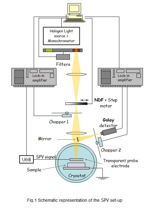
In our set-up for SPV spectral measurements the sample is mounted on a grounded copper platform positioned in a Leybold-Haraeus continuous flow optical cryostat (65-300K). A lamp (100 W or 250 W), a SPEX grating monochromator (f=0.25m), and an optical chopper are used to illuminate the sample surface. Two different semitransparent electrodes (probes) are employed. The first one is a gold grid stretched over a metallic frame holder. It is isolated from the sample by an 8 micrometers polyimide sheet, which has an opening 3 mm in diameter used for illumination. The second probe consists of a SnO2 film (which is transparent and conductive) evaporated on the bottom side of a 5x5 mm2 quartz glass. The glass is adjusted so that the SnO2 film softly touches the sample. With this probe the so called soft-contact SPV [2] measurements can be performed, which allow achieving nearly unity voltage transfer ratio between the sample and the probe. This regime is suitable for measurements of nanostructures, where the signal is usually weak. In both cases the probe signal with respect to ground is fed to a high-impedance unity gain buffer and then measured by an SR830 Lock-in amplifier. The overall system is controlled by a computer. Typical sample dimensions (which fit in the sample holder) are between 5x5 and 10x10 mm2.
The SPV amplitude A and phase φ are determined from the signal in phase (X) with the reference signal and that shifted in phase by 90o (Y) as follows. A = (X2 + Y2)1/2 and φ = arctg (Y/X) . Taking into account the signs of X and Y and the periodicity of the arctg function we obtain φ between –180o and +180o.
The measurements can be performed at a temperature between 65 and 300K with incident light chopped at a frequency between 3 and 3000 Hz. The light wavelength can be scanned in two ranges: from 1800 towards 800 nm and from 900 towards 500 nm using two different gratings (600 and 1200 gr/mm, respectively) and optical filters to cut the high order diffraction. The minimum wavelength step is 0.5 nm. With the 1200 gr/mm grating and 0.25 mm slits the resolution is 1 nm. The maximum photon flux density Ф is around 5x1014 cm-2s-1. The value of Ф is kept constant within ± 0.5 % during the spectral scan. This is achieved by real time regulation of Ф by means of a spectrally flat detector (Goley detector) to monitor the light intensity changes and a neutral density filter driven by a step motor.
The set-up for SPV measurements is represented schematically on Fig.1. The requirements for the sample (or the best sample for SPV) can be found here.
Photoconductivity spectroscopy
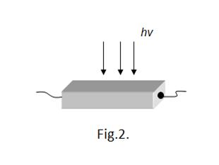
For photoconductivity (PC) spectral measurements we use the same set-up as for SPV. In this case the sample is mounted on an insulating platform. No semitransparent electrode is necessary, but two electrical contacts on the two sides (left and right) of the sample. It is preferable the contacts to be Ohmic. The illumination is from the front side (Fig.2).
Both dc (continuous light) and ac (modulated light) PC can be measured. For dc PC we use a Hewlet-Packard Mod.4140 pA-meter, which incorporates a dc voltage source. For ac PC the same voltage source is used together with a SR830 or EG&G 5207 Lock-in amplifier. Typical sample dimensions (which fit in the sample holder) are 10x5mm2.
[1]. L. Kronik, Y. Shapira , Surface Science Reports. 37 (1999) 1-206.
[2] S. Datta, S. Ghosh, and B. M. Arora, Rev. Sci. Instrum. 72, 177 (2001).